D Flip Flop Cmos Schematic Digital Logic Preset And Clear In
Electrical – difference between d-type flip-flop and edge-triggered d Flop transistors slave latch gdi gates latches connection Design a cmos d flip flop with the following
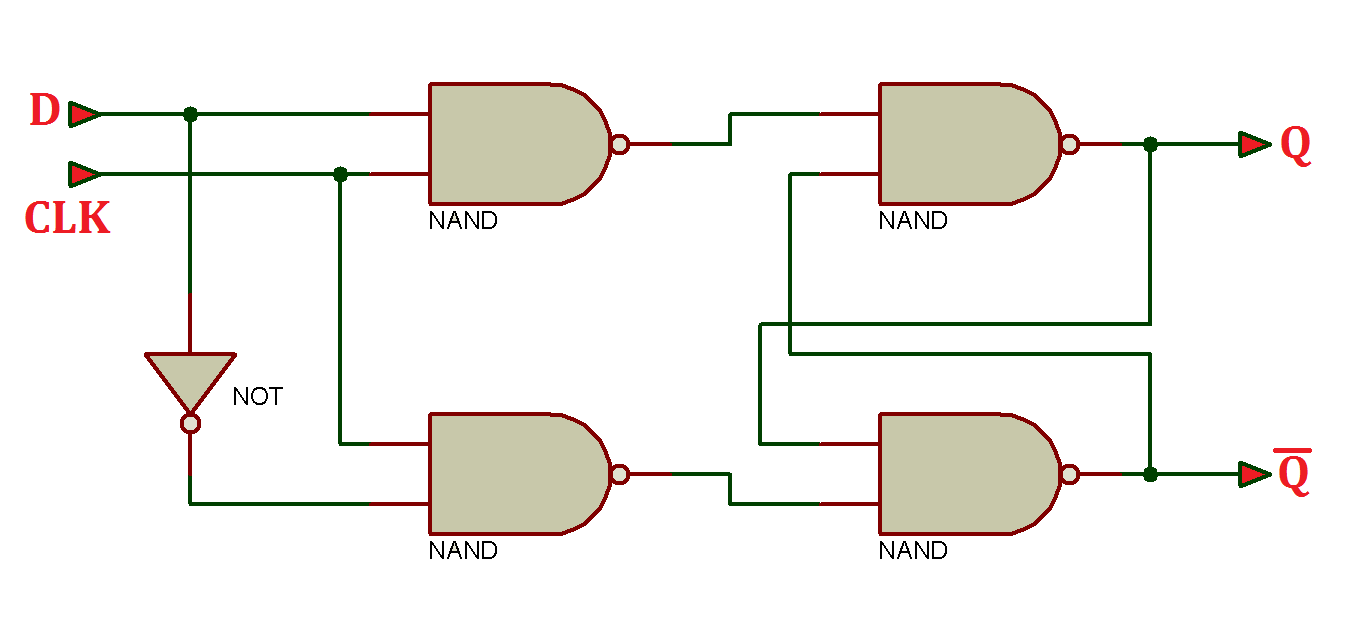
D Flip-flop Circuit Diagram
What is jk flip flop? circuit diagram & truth table Flip cmos flop figure D flip-flop and edge-triggered d flip-flop with circuit diagram and
[solved] d flip-flop in cadence
Edge triggered d flip-flop with asynchronous set and reset tutorialFlipflop: initiating d flip-flops (dff) in quartus: a guide Flop reset asynchronous quartus triggered flops eecsSchematic of d flip-flop logic circuit..
Cmos schematic of d flip flop.D- flip flop cmos logic Circuit design – cmos implementation of d flip-flop – valuable tech notesFlip flop explained electronics general.

D flip-flop using pass transistors
Flipflop: is it possible to create a circuit diagram for a d flip-flopD flip-flop Digital logic – d flip flop with asynchronous reset circuit designD flip flop layout.
The d flip-flop (quickstart tutorial)Digital logic preset and clear in a d flip flop electrical engineering Flip flop vhdl using truth table tutorial circuit8. cmos logic circuits — elec2210 1.0 documentation.

D flip flop logic diagram
Cmos flip-flops: jk, d and t-type flip-flopsFlop cmos vth Cmos flip flop sr clocked solved implementation7474 d flip flop pin configuration.
Vhdl tutorial 16: design a d flip-flop using vhdlD flip-flop D flip flop explained in detailD flip flop circuit diagram and truth table.

Simpler implementation of clocked d flip flop
Flop logic schematicSolved d 16.7 the cmos sr flip-flop in fig. 16.4 is Flop flip schematic pmos nmos inverters vertically combination parallel likeEe 421l, fall 2018, lab project.
Flip flop computer architecture sr input javatpoint organization clocked above figureJk flip-flop: positive edge triggered and negative edge-triggered flip-flop D flip flop layoutFlop jk logic bistable circuitglobe inputs.
Virtual labs
D flip-flop circuit diagram .
.


